
Un site utilisant Réseau de sites JRP - LNE
Micro- and nano-electronics are considered by the European Commission (EC) a Key Enabling Technology (KET) with high potential for innovation throughout the economy, currently accounting for 10 % of EU Gross domestic product (GDP), and fostering highly skilled employment. A competitive advantage in the semiconductor industry is gained through the exploitation of new materials and processes, translating into improved component performance. This requires a metrological infrastructure allowing reliable nanoscale characterisation of new materials and devices, particularly in terms of their electrical parameters and properties. The development of electrical nanoscale metrology has also been clearly identified in the Nano‑electronics Standardisation Roadmap by the International Electrotechnical Committee (IEC-TC113).
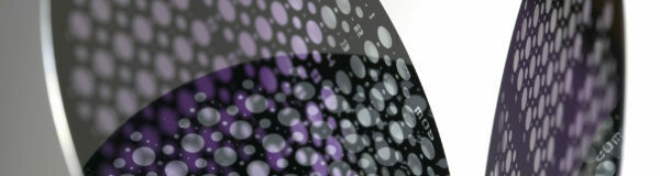
The main metrological problem is the traceability and reliability of measurements of electrical properties at the nanoscale using C‑AFM and SMM. As scanning probe microscopy methods, C‑AFM and SMM are particularly attractive for use in the characterisation of electrical properties at the nanoscale because they allow non‑destructive analysis of electrical components. However, currently most measurements are taken with different instruments or using different reference standards and cannot be compared to each other nor used for modelling. This problem is compounded by a lack of established measurement protocols and a lack of easy to use reference standards. Furthermore, end users need best practice guides, worked examples, and access to easy to use 3D models to assess the influence of environmental conditions, the influence of the particular instruments used in the measurement, and the type of standards used. With these influencing factors, a simplified uncertainty budget can be established for the setup used for the measurement, which is a requirement in many quality standards. Additionally, to make measurements economically viable end users also require cost effective instrumentation, particularly for high frequency measurements.
The overall objective of the project is to establish a European metrological infrastructure and cost-effective technologies for C‑AFM and SMM to allow industry to conduct traceable measurements of electrical properties on materials and devices at the nanoscale.
This EURAMET joint research project is receiving funding from the Horizon 2020 European Union Funding for Research & Innovation under the European Metrology Programme for Innovation and Research (EMPIR).
EMPIR is the main funding programme for European research on metrology. It coordinates research projects to address grand challenges, while supporting and developing the SI system of measurement units.
This project is running from September 2021 to August 2024. It involves 7 National Metrology Institutes, 1 standardization company, and 5 academic organisations:
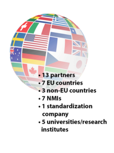
The 7 National Metrology Institutes:
A standardization company:
The five universities/research institutes: